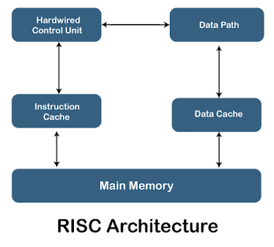
Design a 8 or 16 bit RISC processor with 3 or 4 step pipeline that can do basic arithmetic and logical operation.
1) Instruction set -
The first step in design of a RISC processor is the design of instruction set. An instruction set contains instructions supported by the processor. Load instruction reads data from memory and writes it to a register. If the address of memory location is specified in load instruction, the instruction length will exceed the number of bits used to address memory. An alternative to this is, to write the memory address in a register and specify the register in the instruction. In addition to this, if an offset is specified in the instruction then an operand at a known offset from a memory location can be accessed. So, load instruction capable of copying data from the memory location whose address is sum of base register (Rs) content and offset (Imm) to a destination register (Rt), was selected. Store instruction capable of copying data from register (Rt) to the memory location whose address is sum of base register (Rs) and offset (Imm), was selected. Arithmetic and logical instructions process data present in registers. Both arithmetic and logical operations produce a result after processing two operands. In two operands arithmetic and logical instructions one of the two source registers is the destination register.
2) Instruction format-
The second step is design of instruction format. Each instruction is assigned a unique code, known as operation code (Opcode). For eight instructions 3 bits opcode field is required. The opcode field can be reduced to 2 bits by using same opcode for arithmetic and logical instructions and another code, known as function code, to specify the intended arithmetic or logical operations. For five arithmetic and logical instructions 3 bits function field is sufficient. Each register, in register file, is assigned a unique address. To address eight registers,3 bits address field is required. The systematic placement of these fields in the instruction is referred to as instruction format.
For arithmetic and logical instructions, an opcode field, three 3 bits address fields and a function field
is required. The resulting instruction format is known as R form
3) Datapath and control-
The third step is design of datapath and control unit. Datapath is a systematic arrangement of hardware components and their interconnection for performing an operation. The instruction set is divided into two or more parts with each part containing instructions which require the same logic or hardware for implementation. In this case the instruction set is divided into three classes, arithmetic and logical, memory reference and branch instructions. The datapath for each instruction class is designed and combined to get the final datapath. While combining datapaths a hardware resource is shared by using multiplexer at its input.
For each instruction to perform the expected operation control signals are required. The control signals
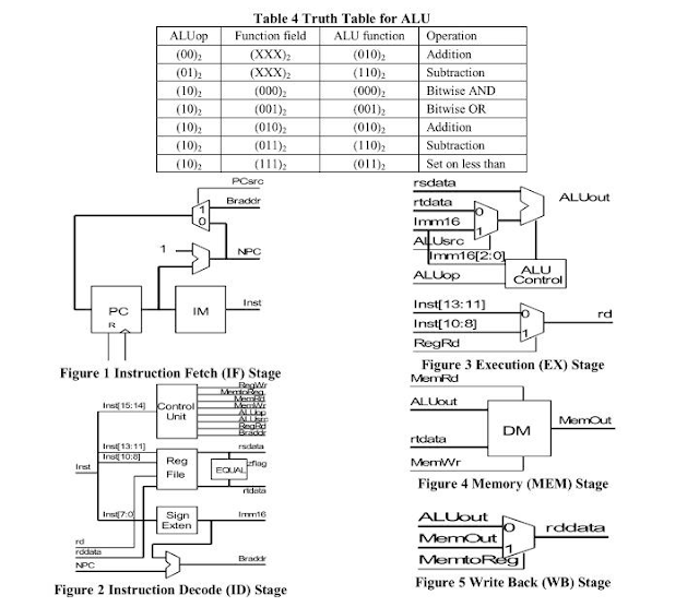
required and the function performed by them is listed in table 2. Control signals are generated by the control unit according to the opcode of instruction. The value of control signal for each instruction is listed in table 3. The ALUop control signal and function field in instruction are used to generate ALU function select signal. The truth table for ALU function select signal is shown in table 4. Depending on the operation performed by each section of datapath, during execution of an instruction, the datapath can be divided into five stages. The five stages are, instruction fetch (IF) (Fig. 1), instruction decode (ID) (Fig. 2), execution (EX) (Fig. 3), data memory access (MEM) (Fig. 4) and write back (WB) (Fig. 5) stage. The operation of each stage was verified by writing VHDL code and simulating it using ISE simulator [2]-[3]. The propagation delay of each stage, as observed in Post Route simulation, is listed in table 5.
4) Pipelining is an implementation technique in which multiple instructions are overlapped in execution. The datapath is pipelined by inserting a register, known as pipeline register, between two stages. The stage enclosed between two pipeline registers is known as pipe stage. The PC and pipeline registers are driven by the same clock and reset signal. For pipelined datapath to work properly, clock with period greater than or equal to maximum of propagation delays of pipe stages, is required. For this processor, according to table 5, the minimum clock period is 20 ns. Problems associated with pipelined datapath are referred to as pipeline hazards. Data dependence between instructions results in data hazards. Data hazards are solved by compiler by inserting no operation (NOP) instruction between the instruction producing the result and the instruction using it. In hardware, techniques like forwarding and stalling are used. In data forwarding, the data forwarding logic creates a path from the location in the pipeline where the required data is available to the location where it is required. In stalling, the hazard detection logic detects data hazard and stalls the pipeline. In case of branch instructions, the delay in starting execution of instruction at branch target address, when branch condition is true, results in control hazards. This delay is reduced by modifying the datapath. VHDL codes for pipelined datapath, pipelined datapath with forwarding logic, pipelined datapath with forwarding and stalling logic, and pipelined datapath modified to handle control hazard were written and tested.
5)The processor was implemented in XC3S400 FPGA. The device utilization is presented in table 6. The XC3S400 development board, from Mechatronics, has 16 input pins, 16 output pins, 4 seven segment LED displays, RS232 interface, USB interface, VGA interface, ADC and DAC. A memory mapped input port at address 8, memory mapped output port at address 9, 4 digit multiplexed display controller and serial transmitter were added to the design. The 4 digit multiplexed display controller was used to display the current instruction fetched from IM (Fig. 6). The serial transmitter was used to transmit, PC contents, instruction fetched, next PC calculated, Rs contents, Rt contents, Imm16, ALU output, ALU output bypassed, memory output, end of line indicator (33), carriage return and line feed, during each clock cycle with 8-N-1 format and 4800 bps. Before transmitting the 16 bit data, it was divided into four 4 bit data and each 4 bit data was converted from binary to ASCII. A test code (table 7) containing the instructions supported by the processor was written to IM, to test the processor. This code contains both data hazard and control hazard. The data obtained in hyperterminal clearly indicates the activities inside the processor. The data dependency between the first and second instruction and fourth and fifth instruction stalls the pipeline. Stalls and one clock cycle branch delay are indicated by square.
Here is 16 bit RISC processor with 5 step pipeline that can do simple arithmetic and logical operation.


